Photoluminescence

PLus-Spot

Photoluminescence testing over large areas

The PLus-Spot system enables the imaging of defects and non-uniformities in solar panels (partially processed or finished) in a fast, non-contact mode

  • No need to connect and disconnect cables for testing
  • No operator needed
Photoluminescence image of back contact solar panel
  • Industrial camera(s), lens(es), and filters customized  for each use case (semiconductor band gap, test area, desired resolution)
  • Array of heat-sinked LEDs (UV, blue, green, red or NIR depending on application) 
  • Programmable power supplies) to drive LEDs
  • Enclosure to support LEDs, to improve light intensity and uniformity, and to eliminate room light artifacts
  • Customized metal frame to support the structure over/under a factory transport system or over a table
  • Optional cables and power supply for EL testing
  • Rack to hold power supplies
  • IMPEL software on a Windows Computer 
  • No-charge software upgrades and usage assistance for two years

Camera: 

  • Resolution: 20-62 MP each
  • Lens: 8-35 mm
  • Filters: Customizable longpass and bandpass wavelengths available 

PL Power Supplies:

  • Input Voltage Range: 208-240V AC 50/60 Hz 

Light Enclosure: 

  • Exterior: Variable
  • Minimum image area: 40 cm x 60 cm (see CellSpot for smaller areas)
  • Maximum image area: 250cm x 130 cm
  • Uniformity of light intensity: Better than 80%
  • Light intensity: Up to 1 Sun

Optional EL biasing

  • Any desired current, voltage, and power

Tower Computer: 

  • Processor: AMD Ryzen 7 7800X3S 
  • Storage: 1 TB 

Throughput: 

  • Generally 3-12 seconds per panel + transport time

Thin film production quality control

Gain feedback on film quality after each processing step for statistical process control.  Perovskites, CdTe, CIGS.  Superstrate or substrate type.

  • After absorber deposition
  • After transport layer or buffer layer deposition
  • After TCO deposition
  • See shunts and non-uniformities
  • Degradation tests
    1. UV or visible light soaking
    2. Collect a series of images vs time

BIPV and VIPV Applications

For Building-Integrated and Vehicle-Integrated PV and other application that involve buying panels and integrating them into structures

  • Test purchased panels to see cracked cells prior to integration
  • Test after integration

Satellite PV Applications

  • Test purchased panels prior to integration for cell/CIC cracks
  • Test panels midway during production
  • Test panels after mounting when contacting strings for EL is difficult or not possible

Need a Custom Solution?

Whether you’re testing next-gen tandem cells, working in a space-rated clean room, or need custom optics for your line, we can help. BrightSpot has built custom EL, PL, and UVF systems for some of the most demanding PV applications on Earth—and in orbit.

Contact us and discuss your needs with one of our experts.

Custom Solution

Download Product Brochure

Download the product brochure to get all the info and specs

IMPEL Software

Control

IMPEL is the unified control platform for BrightSpot imaging systems, enabling seamless coordination of camera, light sources, and power supply. From a single interface, users can adjust exposure settings, trigger PL or EL sequences, and automate capture workflows across multiple system components.

Enhancement

Built-in image processing tools help users sharpen contrast, highlight defects, and visualize subtle variations in cell or panel performance. With support for custom filters and multispectral imaging, IMPEL ensures every captured frame delivers actionable insights, whether in R&D or field diagnostics.

Report

IMPEL simplifies documentation by generating detailed reports with embedded images, metadata, and measurement context. Export results for internal QA, client acceptance, or long-term traceability – standardized and ready to share.
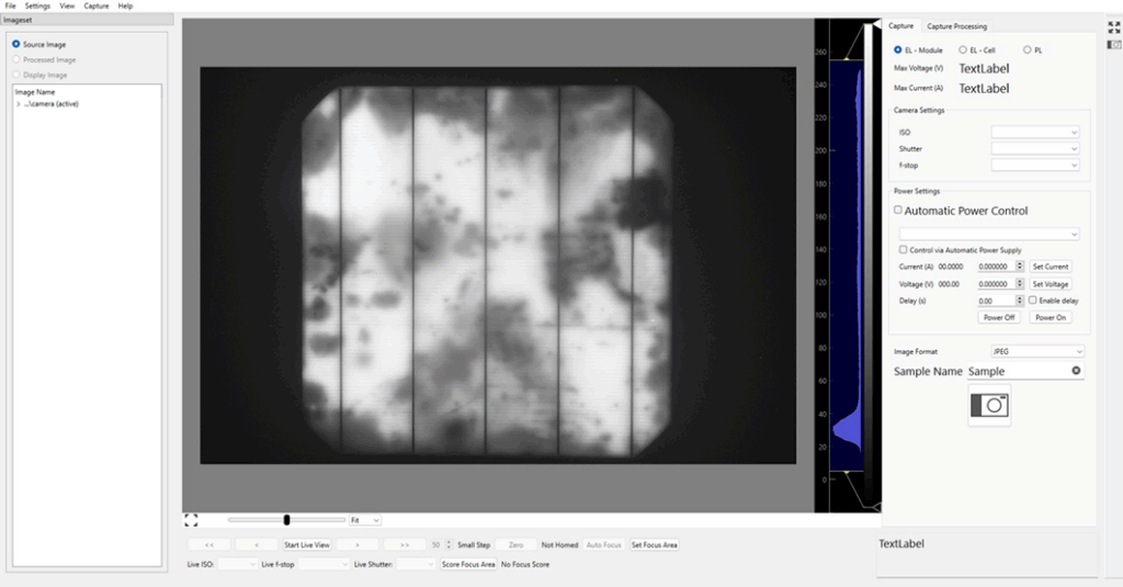
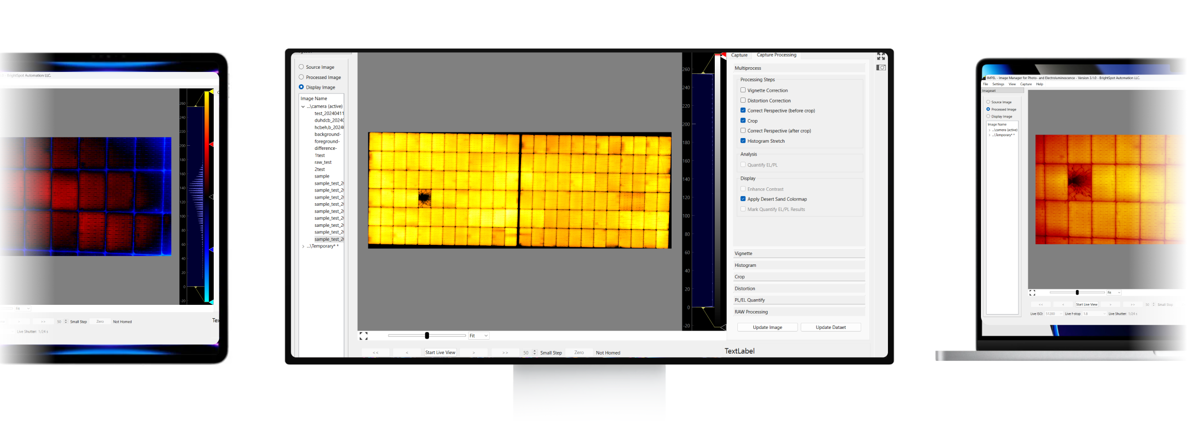
IMPEL Software
IMPEL Software Preview

Publications

Here you’ll find white papers, case studies, and expert commentary designed to provide practical takeaways for professionals and decision-makers

Customized Defect Imaging Solutions for Perovskite and Tandem Cell/Panel Architectures

UV Fluorescence Imaging Of Defects And Bill Of Materials Variations In Bifacial Solar Panels

EUPVSEC – Bilbao, Spain – Sep 22, 2025

Ultraviolet Fluorescence Imaging for Photovoltaic Module Metrology: Best Practices and Survey of Features Observed in Fielded Modules

IEEE Journal of Photovoltaics ( Volume: 15, Issue: 3, May 2025)

Low-Cost Daytime Electroluminescence Imaging

NREL PV Reliability Workshop – Lakewood, CO USA – Mar 6, 2025

UV Fluorescence Imaging for Solar Panel Product Development and Durability Testing

NREL PV Reliability Workshop – Lakewood, CO USA – Feb 28, 2024

Unveiling the Unseen: Harnessing UV Fluorescence for Comprehensive Rooftop PV System Assessment and Successful Insurance Claims Process

NREL PV Reliability Workshop – Lakewood, CO USA – Feb 28, 2024

Detection and Impact of Cracks Hidden Near Interconnect Wires in Silicon Solar Cells

50th IEEE PVSC, Jun 12 2023